
Japan makes some of the world’s most important chip machines and materials, but today it makes no leading-edge logic chips at all. The government is spending several trillion yen to change that, through a start-up called Rapidus and through subsidies for TSMC, Micron and Kioxia factories. This article explains what is being built, how much public money is involved, what the node names such as “2 nm” really mean, and where the risks are. Facts are separated from plans and forecasts. All figures are as of 10 November 2026.
How this relates to other posts: Our 4 November article, Japan’s Chipmakers in the AI Boom, introduced the supply chain (Tokyo Electron, Advantest, Renesas, Sony and others). Our companion article published today, AI Chips and Data Centers in Europe and Japan, covers data centers. Here we focus on the fabs.
Currency note: Yen amounts come from the sources cited. Dollar figures are rounded and use the rates in those sources (roughly ¥155–160 per US dollar).
The short version
- Rapidus (Hokkaido) aims to start 2 nm mass production in the second half of Japan’s fiscal year 2027 (October 2027–March 2028). On 10 November 2026 Bloomberg reported, citing unnamed people, that it has not yet produced working 2 nm SRAM memory cells, is at least months behind and may miss the March 2028 deadline. Rapidus says it remains fully committed to the schedule.
- TSMC’s Kumamoto subsidiary (JASM): Fab 1 has produced chips since late 2024 on mature nodes. Fab 2 was switched from 6/12 nm to 3 nm, with a plan certified by METI on 16 October 2026 and production targeted for 2028.
- Micron Hiroshima broke ground on a ¥1.5 trillion expansion for advanced DRAM and HBM in July 2026; tools arrive in the second half of 2028.
- Kioxia opened a second plant in Kitakami for 3D flash memory in September 2025.
- “2 nm” is a name, not a measurement. No part of a 2 nm chip is 2 nm in the way the name suggests.
What “2 nm” really means
A nanometre (nm) is one billionth of a metre. A human hair is very roughly 70,000 to 100,000 nm thick, and a silicon atom is a fraction of a nanometre across. So “2 nm” sounds like transistors a few atoms wide.
It is not. For decades the node name did describe a real size, roughly the length of the transistor’s gate. That link broke in the 1990s; Wikipedia’s summary of the industry roadmaps says that since about 1994 the number “has become more of a marketing term that has no standardized relation with functional feature sizes or with transistor density.” Today a node name is a label for a generation: “3 nm” is newer, denser and more efficient than “5 nm”, but neither number is a ruler reading.
IBM, which developed the 2 nm technology that Rapidus licenses, says so itself. In its research blog on its 2021 2 nm chip, IBM writes that “2 nm does not correspond to half pitch of contacted metal wires, as traditionally defined,” and compares node names to “5G”: a label for a generation, not a physical size.
The distances that actually matter
Chip designers care about pitch: the distance from the start of one repeating feature to the start of the next.
- Contacted gate pitch (CGP): the spacing between neighbouring transistor gates, in effect how tightly transistors are lined up in a row.
- Metal pitch: the spacing between the thinnest copper wires that connect transistors.
- Gate length: the length of the gate that switches the transistor on and off.
According to the 2021 update of the IEEE’s International Roadmap for Devices and Systems (IRDS), as summarised on Wikipedia, a node labelled “2.1 nm” was projected to have a contacted gate pitch of about 45 nm and a tightest metal pitch of about 20 nm:
| Node label | Gate pitch (IRDS projection) | Tightest metal pitch (IRDS projection) | Year |
|---|---|---|---|
| 7 nm | 60 nm | 40 nm | 2018 |
| 5 nm | 51 nm | 30 nm | 2020 |
| 3 nm | 48 nm | 24 nm | 2022 |
| “2 nm” | 45 nm | 20 nm | 2025 |
| 1 nm | 42 nm | 16 nm | 2027 |
These are roadmap projections, not any company’s measured numbers, and individual companies differ. IBM’s 2021 chip, for example, reported a 44 nm contacted poly pitch and a 12 nm gate length, which IBM described as “just two dozen atoms long”. Note the point: a label of “2” sits next to a gate pitch around 44–45 nm and a gate 12 nm long. The label is about 20 times smaller than the real spacing.
Another way to compare is transistor density: how many transistors fit into one square millimetre. IBM said its 2021 chip could hold up to 50 billion transistors on a fingernail-sized chip. A technology analyst later computed from an IBM-confirmed area of 150 mm² that this equals roughly 333 million transistors per mm². Different companies’ “2 nm” processes also differ in density, which is why comparing names across companies is unreliable. As Wikipedia notes, Intel’s older “10 nm” process was similar in density to TSMC’s “7 nm”.
What is actually new at “2 nm”: the gate-all-around transistor
Earlier “FinFET” transistors have the gate wrapped around three sides of a vertical fin. The new design, gate-all-around (GAA) nanosheet transistors, stacks thin horizontal sheets of silicon and wraps the gate around all four sides. Better gate control means less current leaking when the transistor is off. TSMC’s “N2”, which it says entered high-volume manufacturing in the fourth quarter of 2025, is its first nanosheet process. TSMC states that versus its “N3E” it offers up to 15% higher speed at the same power, or up to 30% lower power at the same speed, and more than 1.15 times the chip density. Samsung and Intel have comparable gate-all-around processes; Intel markets its as “18A” (1.8 nm-class), which, per Wikipedia, entered volume manufacturing in late 2025. So “2 nm” already exists in volume at three companies. Rapidus is trying to become the fourth.
Why EUV and SRAM come up so often
Two technical terms recur in the Rapidus story:
- EUV (extreme ultraviolet) lithography: machines made by the Dutch company ASML that print the finest patterns with very short-wavelength light. Rapidus installed Japan’s first volume-capable EUV system (an ASML NXE:3800E) in December 2024.
- SRAM: the small, very fast memory built into every processor from the same transistors. A modern chip contains many millions of SRAM cells. If a new process cannot make SRAM cells that work reliably, it cannot make a usable processor, which is why SRAM is a standard early test of a new process.
Rapidus: the 2 nm bet in Hokkaido
Who and what. Rapidus was founded in 2022 with money from eight Japanese companies (Kioxia, Sony, SoftBank, Denso, Toyota, NEC, NTT and MUFG Bank), plus government backing. It signed a technology partnership with IBM in December 2022 and sends engineers to IBM’s research centre in Albany, New York. Its factory, IIM-1 (“Innovative Integration for Manufacturing”), is in Chitose, Hokkaido, close to New Chitose Airport.
Timeline according to Rapidus and press releases:
- September 2023: groundbreaking.
- December 2024: first EUV machine installed.
- April 2025: pilot line begins operating.
- July 2025: Rapidus announced that prototype 2 nm gate-all-around transistors showed working electrical characteristics. This is an early step, far from a working chip.
- Late 2026 / early 2027: according to an interview with Rapidus’s chief technology officer in Nikkei xTECH (19 February 2026), a shuttle service producing customer-designed test chips was to start, and version 1.0 of the process design kit (PDK, the rulebook chip designers use) was due around the end of 2026 or early 2027, after an improved “0.5” version from May–June 2026.
- Second half of fiscal 2027: planned start of mass production.
- Around fiscal 2029: break-even operating cash flow; about fiscal 2031: stock market listing (both from the government’s plan, as reported by EE Times Japan and Nikkei).
Manufacturing approach. Rapidus says it processes wafers one at a time (“single-wafer processing”) in the front-end steps, which it argues allows faster feedback and tuning than the conventional method of processing wafers in batches.
The expansion plan is unconfirmed. Reports in November 2025 said Rapidus wanted a second Hokkaido plant for 1.4 nm chips from 2029. We did not find an official construction schedule for a second plant, so treat it as an ambition.
The money: what the state has committed
Japan treats Rapidus as a matter of economic security. The main numbers:
- Research and development support: the economy ministry (METI) approved a further ¥631.5 billion (about $4 billion) in April 2026, bringing approved R&D support to ¥2.354 trillion (about $15 billion), according to Reuters. The money flows through NEDO, a government research agency. METI also lists a request of about ¥300 billion for fiscal 2027.
- Government equity: the state, through the Information-technology Promotion Agency (IPA), has put in ¥100 billion in fiscal 2025 and ¥150 billion in fiscal 2026. On 19 October 2026 METI presented a plan to add ¥400 billion over fiscal 2027–2029 (¥150 billion, ¥150 billion and ¥100 billion), which would bring state equity to ¥650 billion. This is not yet approved; each year needs a budget decision. (EE Times Japan, 20 October 2026.)
- Private money: in February 2026 Rapidus announced about ¥268 billion in new equity from the government and 32 companies, including Canon, Fujitsu, Honda and several banks (MONOist). It aims for roughly ¥1 trillion in private equity over fiscal 2025–2031.
- Bank loans: Rapidus plans ¥2 trillion (about $13 billion) in loans from private banks, with state debt guarantees. So far only non-binding letters of intent exist, according to METI documents reported by EE Times Japan. The government’s extra equity is meant to keep Rapidus’s balance sheet strong enough for those loans.
Put together, public support is reported to have passed ¥2 trillion already, and Asahi Shimbun, as relayed by Seoul Economic Daily, said it could reach ¥3.2 trillion by 2029 if the plans are approved. The 2024 Japanese policy of mobilising more than ¥10 trillion for AI and chips by fiscal 2030 is the wider frame; we did not check how much of that has been spent.
Customers and the 10 November report
Customers. Rapidus says it is discussing business with more than 60 companies, has given rough quotes to about ten and was preparing to license its design kit to them (MONOist, March 2026). Reuters reported that Rapidus signed 17 chip-design partners, including Synopsys, Cadence, Infosys and Toppan, but, as of that report, no named production customer. The trade outlet Electronics Weekly reported in March 2026 that Canon would order 2 nm test chips (designed using Synopsys software) from Rapidus. That is a test order, not a volume contract. IBM is a technology partner and Tenstorrent a joint-development partner; neither is a confirmed volume customer. “Who will actually fill the fab” is, in the words of one investment director quoted by Reuters, the biggest question.
Bloomberg, 10 November 2026. Bloomberg reported, citing people familiar with the matter, that Rapidus:
- has not yet produced functioning 2 nm SRAM cells, a step that was supposed to be done by this summer;
- is therefore “at least months behind schedule”, and may no longer make its pledge of mass production by March 2028;
- is still working on dust and particle control in its cleanroom; and
- may ultimately succeed after some years’ delay, according to those people.
Rapidus’s response, per Bloomberg: it “continues to devote its full efforts toward the start of mass production in the second half of fiscal 2027”, and it declined to give technical details, calling them confidential. Bloomberg adds that an expert panel commissioned by a government agency reported in September that development is progressing, that Economy Minister Ryosei Akazawa said last month the government is ready to keep supporting Rapidus until it is financially viable, and that a delay could also push back the listing goal. TrendForce, relaying the report, points out that since the July 2025 transistor announcement, publicly disclosed progress has mostly been design-kit releases.
How to read this. It is a report from anonymous sources; the company has not confirmed the details and has not disclosed its own technical status. SRAM is a standard early test, as explained above, so a delay there matters, but we cannot judge from outside how large the gap is. The thing to watch is official evidence of working customer test chips from the shuttle run planned from late 2026.
TSMC in Kumamoto (JASM): the foreign anchor
Japan Advanced Semiconductor Manufacturing (JASM) is TSMC’s majority-owned Japanese subsidiary; Sony, Denso and Toyota are among the minority partners.
Fab 1 (running). TSMC’s 2025 annual report says the first Kumamoto fab began volume production at the end of 2024 with very good yield. It was designed for mature “specialty” processes (originally 12 to 28 nm) for cars, industrial machines and image sensors. A trade report that cites EE Times Japan and Reuters says METI certified a revised plan for Fab 1 on 16 October 2026, with main products now 22/28 nm logic plus 40 nm, and capacity of 50,000 wafers per month (down from 55,000). We read this only in that secondary report.
Fab 2 (under construction, switched to 3 nm). Originally planned for 6/12 nm chips, the second fab is now planned for 3 nm logic, the same “3 nm” generation that TSMC has been producing in Taiwan since 2022. TSMC’s chief executive C. C. Wei told Japan’s prime minister in February 2026 that the change was due to strong AI demand. Reuters reported on 1 April 2026, from a Taiwanese government filing, that equipment installation and mass production of 3 nm wafers were expected in 2028. On 16 October 2026 METI approved the revised plan; according to Digitimes and a Korean trade report relaying EE Times Japan and Reuters:
- Subsidy cap: up to ¥645.15 billion (about $4.1 billion), down from ¥732 billion for the original plan.
- Initial certified capacity: 6,000 wafers per month (300 mm wafers), far below the originally planned 48,000. The Taiwanese economics ministry had cited 15,000 wafers per month in a filing in March 2026, so the final size is not settled and, per reports, depends on further Japanese support in the fiscal 2027 budget.
- Production start by December 2028, with first shipments in the fourth quarter of 2028.
- TSMC said at its 15 October earnings briefing that the project is progressing smoothly, with mass production planned for 2028. Reuters reported TSMC’s combined spending on both Kumamoto fabs would exceed $23 billion.
Why it matters. Fab 2 would be Japan’s first plant for 3 nm chips. Unlike Rapidus, it uses a process TSMC already runs, so the technical risk is lower and the schedule more credible. But it is a foreign-owned factory, and the 3 nm node will no longer be the newest by 2028: TSMC’s annual report lists its next node, “A14”, for volume production in 2028.
Micron Hiroshima: advanced memory with EUV
Micron’s Hiroshima plant makes DRAM, the fast memory used in computers and AI servers, including HBM (high-bandwidth memory), the stacked memory sitting next to AI GPUs. In July 2026 Micron began building a new cleanroom building; the opening phase covers about 28,000 m², with tools to be installed from the second half of 2028. Total investment is reported at about ¥1.5 trillion (about $9 billion). METI announced on 12 September 2025 a subsidy of up to ¥536 billion for advanced memory research, development and production there; Japanese reports put total state support for the site, including earlier rounds, at roughly ¥770 billion. Micron said the expansion would create more than 1,000 jobs. Micron calls its current node “1-gamma”, produced with EUV at Hiroshima.
The names “1-beta” and “1-gamma” are, like “2 nm”, generation labels. DRAM naming dropped real nanometre values years ago.
Kioxia: flash memory by stacking, not shrinking
Kioxia (formerly Toshiba Memory) makes NAND flash with partner Sandisk in Yokkaichi and Kitakami. Kioxia and Sandisk announced the start of operation of Kitakami Fab 2 on 29 September 2025 for “eighth-generation” 3D flash with 218 layers; meaningful output was expected from the first half of 2026. The Japanese government approved up to ¥150 billion in subsidy for the joint venture’s plants in 2024, in addition to up to ¥92.9 billion in 2022. Kioxia’s Q&A says total grants including joint ventures are about ¥240 billion. For flash memory, progress is measured by the number of layers stacked vertically, not by node names. Kioxia makes NAND, not HBM.
Where Japan stands: strategy and risks
The strategy. Japan’s approach has three parts: (1) lure a proven foreign leader (TSMC, Micron) with subsidies; (2) build a domestic leading-edge champion (Rapidus), partnering with IBM and others; (3) keep its strength in tools and materials (see our 4 November article). The stated goal is supply security for cars and industry, and relevance in AI. The “three-layer” idea, with Kioxia’s flash, Micron’s DRAM and Rapidus’s logic all in Japan, is discussed by industry commentators, but we found no official three-company alliance.
The risks, in plain words.
- Technology risk (Rapidus): the Bloomberg report suggests the hardest part, making all parts of a new process work together at high yield, is not yet solved. A related disagreement was also reported: an outside director mentioned a yield target of at least 80%, while the CEO and another executive said that definition is not shared by all executives.
- Customer risk: without large named customers, a fab cannot repay its cost. Competitors TSMC, Samsung and Intel already offer 2 nm-class processes. Some likely buyers told Reuters they could not move all their work away from TSMC.
- Money risk: the plan needs private equity and ¥2 trillion in bank loans on top of state aid; the extra ¥400 billion in state equity is still a request.
- Dependence on TSMC: even a successful Japan still relies on TSMC and on imported tools.
- Local strain: Kumamoto and Hokkaido face pressure on housing, roads, labour and water, as earlier coverage noted; we did not examine this in detail.
- Oversupply risk in memory: trade reports note concern that many new memory plants arriving after 2028 could face weaker demand.
What to watch next
- Late 2026 / early 2027: Rapidus’s customer test-chip shuttle and the PDK 1.0 release; any official comment on the SRAM report.
- December 2026: the government’s budget decision on the ¥150 billion in fiscal 2027 equity and ¥300 billion R&D request for Rapidus.
- Bank loans: whether private banks sign binding loan agreements.
- JASM Fab 2: tool-in timing and final capacity beyond 6,000 wafers per month.
- Micron Hiroshima: equipment installation from the second half of 2028.
- Named customers: any public announcement of a volume customer for Rapidus.
What we could not verify
- Bloomberg’s report is based on unnamed sources; Rapidus has not confirmed or denied details. We did not see an official METI reaction.
- JASM Fab 1’s revised product mix and capacity come from a secondary trade report.
- JASM Fab 2’s capacity: 6,000 (METI, per reports) versus 15,000 wafers per month (Taiwan’s ministry, March 2026).
- Any official plan for a second Rapidus fab (only media reports and an executive’s ambitions).
- Micron’s total state support of about ¥770 billion (Japanese press figure) and the ¥1.5 trillion investment figure (media-reported, not a Micron price tag).
- How much of the wider ¥10 trillion AI and chip package has been spent.
- Node-level metrics (pitches, density) for Rapidus’s own process: none have been published, so the IRDS table is a roadmap, not Rapidus data.
FAQ
What does “2 nm” mean? It is a generation label, not a measurement. The real spacings are much larger: about 45 nm between gates and about 20 nm between the finest wires, according to the IRDS roadmap, and IBM’s 2021 test chip had a 12 nm gate length.
Is a 2 nm chip really made of 2 nm parts? No. A few layers inside a transistor are only a few nanometres thick, but the transistor as a whole, its spacing and its wiring are much larger.
Can I compare Rapidus “2 nm” with TSMC “2 nm”? Only roughly. Names are set by each company. Compare density, speed and power from published data once available. Rapidus has not published density figures.
When will Rapidus make chips in volume? Rapidus’s target is the second half of fiscal 2027 (October 2027 to March 2028). Bloomberg reported on 10 November 2026 that it may miss March 2028; Rapidus says it remains committed.
How much public money has Rapidus received? Approved R&D support totals ¥2.354 trillion (about $15 billion) through fiscal 2026, plus government equity of ¥250 billion, with a further ¥400 billion in equity planned but not yet approved.
What is being built in Kumamoto? Fab 1 (running since late 2024, mature chips) and Fab 2 (under construction, planned for 3 nm from 2028).
Is Micron’s Hiroshima plant a 2 nm fab? No. It makes DRAM and HBM on Micron’s “1-gamma” node; DRAM and logic nodes are not comparable.
Why does Japan want leading-edge chips? The government cites supply security and economic security, and the AI boom. Supporters say it reduces reliance on Taiwan; critics ask whether the cost is justified.
Image credit
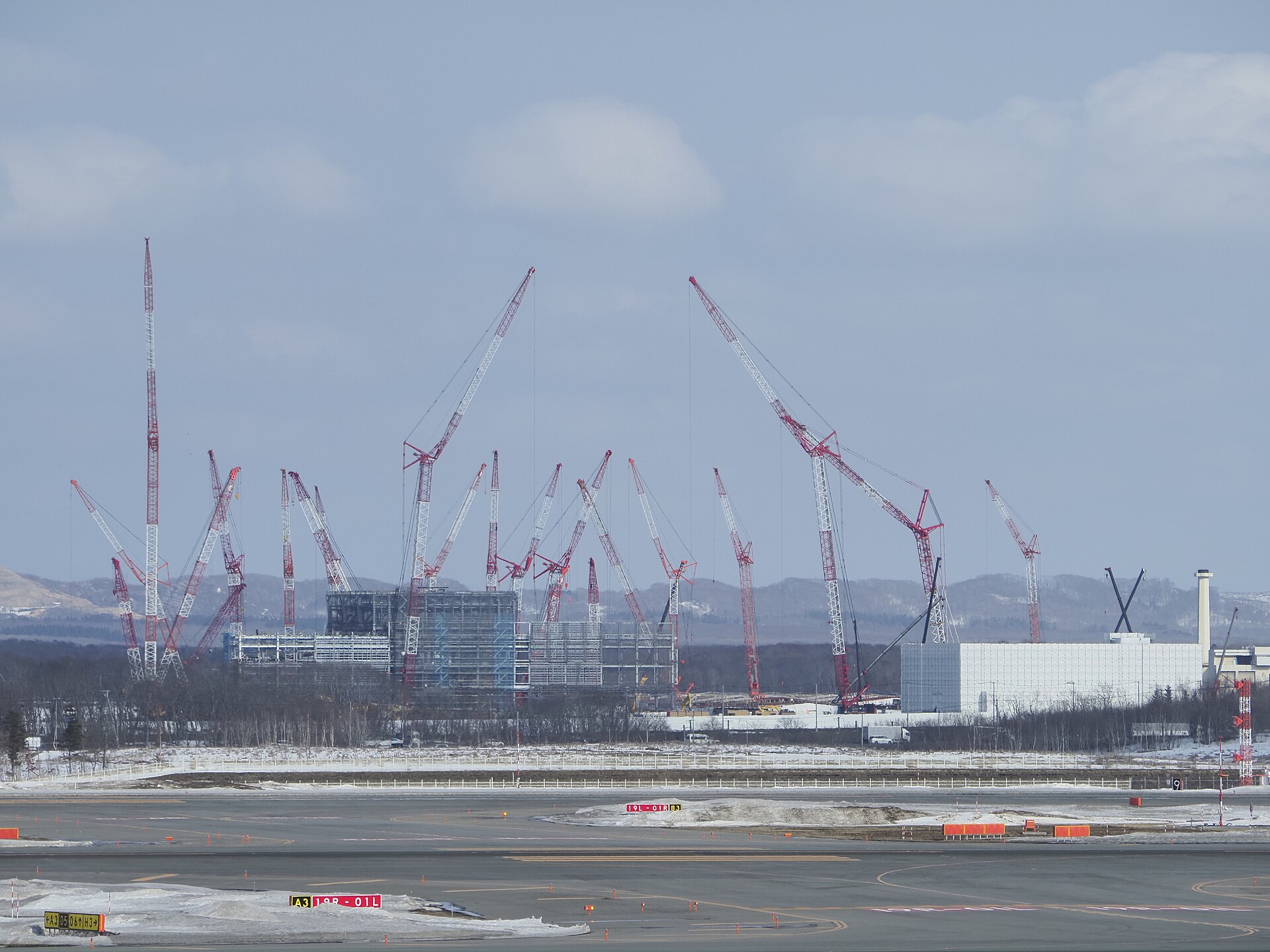
Photo: どういたしまして (Wikimedia Commons user), “Rapidus factory under construction” (14 March 2024), CC BY-SA 4.0, via Wikimedia Commons. The photo shows the site during construction, not any chip or process named here.

Sources
- Bloomberg via The Japan Times: Japan’s Rapidus is said likely to miss mass production deadline (10 Nov 2026) and The Edge Malaysia (full Bloomberg text)
- TrendForce: Rapidus reportedly months behind on 2 nm SRAM (10 Nov 2026)
- Rapidus: IIM (official site)
- Rapidus press release: prototyping of 2 nm GAA transistors (July 2025)
- Nikkei xTECH: Rapidus to produce 2 nm test chips from end of 2026 (19 Feb 2026, Japanese)
- Reuters: Japan approves additional $4 bln for chipmaker Rapidus (11 Apr 2026)
- EE Times Japan: METI reveals ¥400 billion additional equity plan for Rapidus (20 Oct 2026, Japanese)
- Seoul Economic Daily: Japan to inject additional 400 billion yen into Rapidus (20 Oct 2026)
- MONOist: Rapidus funding and customer progress (2 Mar 2026, Japanese)
- Electronics Weekly: Rapidus gets its first customer (9 Mar 2026)
- The Next Web: Rapidus teams up with 17 firms to win customers (citing Jiji and Reuters)
- Digitimes: TSMC’s 3 nm Kumamoto plan wins Japan’s approval (17 Oct 2026)
- VLSI Korea: TSMC Kumamoto Fab 2 moves to 3 nm (relaying EE Times Japan and Reuters)
- Reuters: TSMC plans 3-nanometre chip production launch in Japan in 2028 (1 Apr 2026)
- Taipei Times: Taiwan approves TSMC’s 3 nm upgrade for second Japan fab (1 Apr 2026)
- TSMC: 2025 Annual Report, chapter 1 (PDF) and TSMC N2 technology
- Investment Monitor: Micron starts Japanese chip plant expansion
- TrendForce: Micron breaks ground on Hiroshima fab expansion (6 Jul 2026)
- Mynavi TECH+: Micron Hiroshima groundbreaking (6 Jul 2026, Japanese)
- Kioxia and Sandisk: start of operation of Fab2 at Kitakami (29 Sep 2025)
- Kioxia and Western Digital: up to ¥150 billion subsidy (6 Feb 2024)
- Kioxia: Q&A summary, Corporate Strategy Meeting 2025 (PDF)
- IBM Research: Introducing the world’s first 2 nm node chip (6 May 2021) and IBM newsroom announcement
- Semiconductor Digest: IBM 2 nm GAA-FET technology (gate pitch 44 nm, gate length 12 nm)
- Wikipedia: 2 nm process (summarising the IEEE IRDS 2021 update) and Semiconductor device fabrication
- Postation: Micron Hiroshima and the “three-layer” idea (Japanese)
- Wikimedia Commons: Rapidus factory under construction (image)